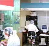
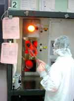
THAT Corporation has long been known in the professional audio marketplace for its high-performance analog integrated circuits. These components are designed to be manufactured using “dielectric isolation” (DI) fabrication, an advanced process technology that provides higher device-to-device breakdown voltages, better isolation between individual transistors, and faster speeds. THAT’s requirements in this area, coupled with the company’s desire to control quality, time to market, and the underlying process variables in all phases of its IC production, led to the acquisition of its own semiconductor fabrication facility in December 1999.
This four-inch wafer fab gives THAT Corporation the only IC production facility focused primarily on high-performance audio components. While this production fab facility primarily produces THAT’s own proprietary product, it is also well suited to service other semiconductor manufacturing needs. Foundry customers are invited to design their own chips on our existing processes or consult with THAT corporation’s fab engineering team to design their own processes. For example THAT’s fab has provided fabricated wafers to the “End of Life” semiconductor market where low production volume, customized processes are typical. THAT has also provided wafer processing services such as thin film deposition or photomasking.
Some of what THAT Corporation offers as foundry services to outside semiconductor customers include;
1. A 40V, fully complementary bipolar process with precision thin-film resistors. This process is based on dielectric isolation (DI), and offers discrete-component performance within an integrated circuit. Inter-device isolation ranges up to 200V.
2. A 40V JI process with vertical NPN’s and Lateral PNP’s. This process can also be fabricated with precision thin film resistors.
3. Thin Film deposition services can be provided on a stand-alone basis. Our precision thin film resistors can be manufactured with high sheet resistance and low TCR. We also offer Aluminum sputter deposition services.
4. Other fab processes; THAT offers a variety of other fab processes including diffusion, photomasking and etching of 100mm wafers.
Because every foundry application is different, we encourage companies who may be interested in our semiconductor fabrication capabilities to contact us directly to discuss whether our process will fit your requirements.
Contact us now to begin discussing your foundry requirements.

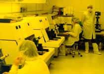
The following is a brief summary of our fab capabilities:
— Wafer size: 100 mm (4 inch wafers)
— Clean room specification: Class 1000 (Class 100 under laminar hoods)
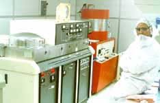
Selected fab equipment:
— Perkin-Elmer projection aligners (capable of 3 micron feature size)
— MRC sputtering machine with 3 target capability (SiCr, NiCr, Al)
— Fully automated Thermco diffusion furnaces with SiC cantilever loading
— Wet and dry etching capability
— KOH-based Anisotropic etch bath for V-groove etching
Contact us now to begin discussing your foundry requirements.

Semiconductor Foundry
Mailing address: 505 Fairview Way, Milpitas, CA 95035 USA
Telephone: +1 (408) 586-8428
Fax: +1 (408) 586-8429
Email: Foundry Information
North America Sales Representative
DAPike Engineering Inc.
Contact: Doug Pike
Phone: +1 541 420 1243
Email: Doug Pike
Web: www.dapikeengineering.com