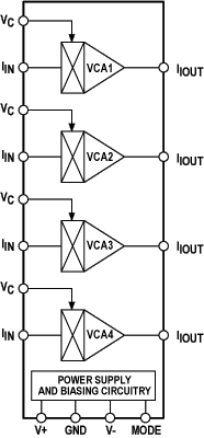
Analog Devices has discontinued their SSM2164 quad VCA. Our THAT 2162 dual VCA is comparable in many respects.![]()
To replace a 2164 with (two) 2162 ICs, see below for some of the issues which you will need to consider. Please contact applications support for specific assistance with the 2162. And, if you want to find out more about the possibility of a THAT equivalent to the SSM2164, please contact our sales department.
| Key Specifications | |||
| Parameter | SSM2164 | THAT2162 | Conditions |
| Dynamic Range | 116 dB | > 118 dB | |
| Gain Range | 120 dB | > 130 dB | |
| THD + N | 0.16 % | 0.05 % | Class A-B, Typical, 0 V control voltage |
| 0.02 % | N/A | Class A, Typical, 0 V control voltage | |
| Noise | -94 dBu | -97.5 dBu | Class A-B, Typical, 20 kHz BW, 0 dB gain |
| -83 dBu | N/A | Class A, Typical, 20 kHz BW, 0 dB gain | |
| C-V Feedthrough | 1.5 mV | 1.0 mV | Class A-B, 0 ~ -40 dB |
| Gain Matching | 0.07 dB | 0.2 dB | Typical, Channel to channel |
| Supply Voltage | ±4 V to ±18 V | ±2.25 V to ±16 V | |
| Supply Current | ±2 mA / VCA | ±3.5 mA / VCA | Maximum, ± 15 V supplies |
| Packaging | Quad | Dual | |
| Packaging / Layout | |
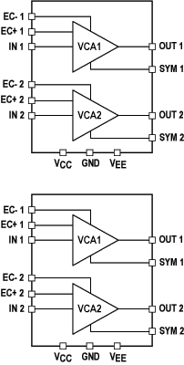
| The THAT2162 IC contains two VCAs, while the SSM2164 has four. So, two 2162s are needed to replace one 2164. However, the 2162 comes in a QSOP16 package, which occupies only 30 square mm of PCB space – about half the space required by the SOIC version of the 2164. Thus, the board space required is a toss up. | |
| SSM2164 | THAT 2162 |
 |
 |
| DIP16, 20mm x 6mm (approx.) = 140 sq mm SOIC16, 10mm x 6mm (approx.) = 60 sq mm |
QSOP16, 5mm x 6mm (approx), x2 = 60 sq mm |
| Control Ports | |||||||||||||||||||||||||||||||||||||||
|
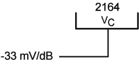
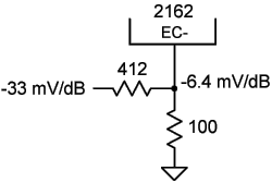
The 2164 has a single control port for each VCA, the 2162 has two ports of opposing polarities. The control constants are different (see table below), so adapting the 2162 to a 2164 application will require circuit changes. Both parts offer 120dB of gain range, but differences in symmetry of that range will be important for some applications. Again, see the table below.
|
|||||||||||||||||||||||||||||||||||||||
| Inputs and Outputs | ||
| Parameter | SSM2164 | THAT2162 |
| Input / Output Current Flow | Current In / Current Out | Current In / Current In |
|
Current in to the input terminal of the 2164 produces current out of the output terminal. As a result, the voltage at the output of the current to voltage converter stage is out of phase with the input voltage. Current in to the input terminal of the 2162 produces current in to the output terminal. As a result, the voltage at the output of the current to voltage converter stage is in phase with the input voltage. This is a significant difference. In some applications, this may necessitate the adding (or removing) an inverter stage when replacing the 2164 with the 2162. |
||
| Parameter | SSM2164 | THAT2162 |
| Input Resistor Value | 30 kΩ | 20 kΩ |
| Current to Voltage Feedback Resistor Value | 30 kΩ | 20 kΩ |
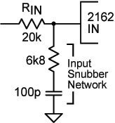
| For best noise performance with the 2162, we recommend 20 kΩ for the input resistor (Rin) and for the output (Rout) resistor in the current-to-voltage converter. Note also the difference in the current to voltage converter frequency compensating capacitor (Cout). Also note the difference in the input snubber network values. | ||
| Parameter | SSM2164 | THAT2162 |
| Input Network Recommended Component Values |
 |
 |
| Current to Voltage Converter Recommended Component Values |
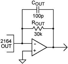 |
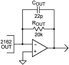 |
| It is OK to use 30 kΩ resistors with the 2162, but the noise performance will be increased by approximately 3.5 dB (at unity gain). | ||
| Operating Mode | ||
| Parameter | SSM2164 | THAT2162 |
| Operating Mode Biasing | Class A or Class A-B, selectable via external resistor | Class A-B only |
| In class A operation, the 2164 provides better THD performance (at unity gain), but it comes at significant expense in noise. Noise increases from -94 dBu to approximately -83 dBu using ADI’s recommended circuit for Class A operation. As well, dc feedthrough is worse — unspecified. THAT believes that class A-B operation offers a better tradeoff in VCA design, so the 2162, like all other THAT VCAs, operates only in class A-B mode. | ||